GHS development memories after all this time
WIRED is committed to establishing laser processing technology that does not exist anywhere else in the world, based on the company philosophy of “building a new world through light.”
We are also working on laser application development while responding to customers’ requests for prototype processing.
We are pursuing a wide range of topics such as micron-level accuracy, optimized energy efficiency for high tact, wavelength, synchronization of laser and stage (roll to roll) and optical scanning, etc.
WIRED’s patented GHS🄬 optical scanning mechanism focuses on “unparalleled hole processing speed.”
The combination of roll-to-roll and lasers has enabled micro hole processing at 100,000 to 200,000 holes/second. However, many obstacles awaited us in the development of this technology.
■Structure Conception
“I know galvanometers and polygon mirrors are too slow and unproductive.”
“Something like that would require a completely different conception of optical scanning technology…”
“Me? I use my hands. I do not use my brain.”
“That is right.”
“How about this?”
(The diagram that the genius suddenly began to draw on the whiteboard was quite strange.)
(It is still fresh in my memory that the genius was a )
(The pinky finger of the hand holding the marker was also standing up.)
Let’s do it, cause it’s fun.” (It was a quick decision.)
- (It was a quick decision.) – After experiencing the hardships of the subsequent development, I have now stopped making quick decisions. –
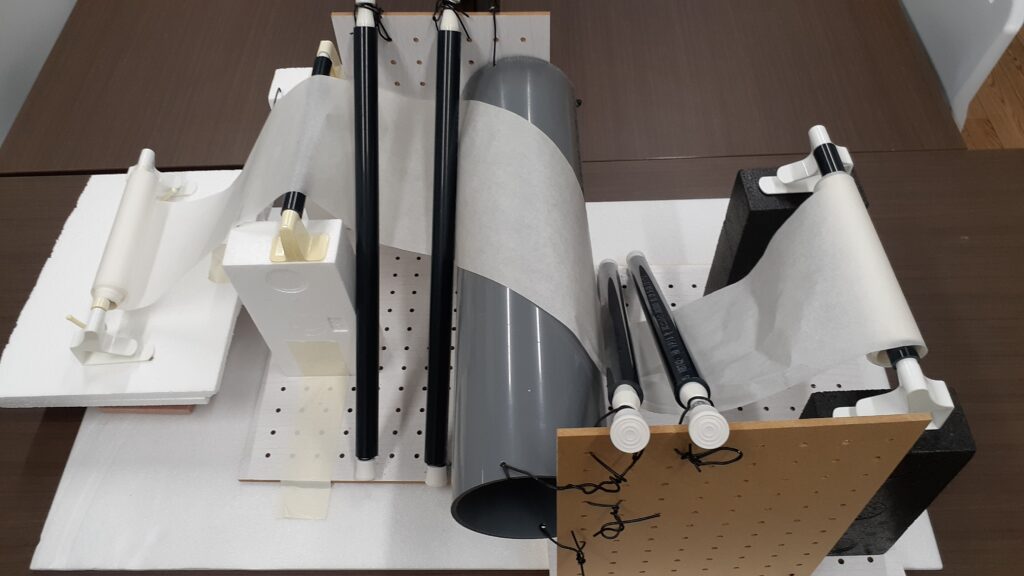
Before considering a new mechanism, a simple mock-up is created to visualize and share the image, and to share the understanding of application development.
We share our understanding not through words or sentences, but by actually seeing things with our eyes to shape the direction of the project. Seeing is believing.
■ Creating a concept model
“I used a 3D printer to make the round one and the complex internal structure.”
“Let’s see…”
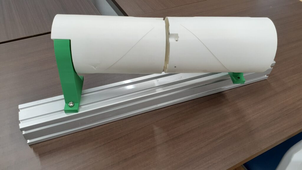
“Ilike it. But… can you make this shape with anything other than a 3D printer?”
“Ummm… I will see what I can do.”
Although concept models tend to be filled with ideals, we will discuss the processing method, cost, overall product accuracy when combining individual components, process structure, and verification methods for actual product manufacturing, not only with lasers, but also with experts in various fields, to come up with a more realistic and inexpensive method.
■Production of prototypes built into actual machines
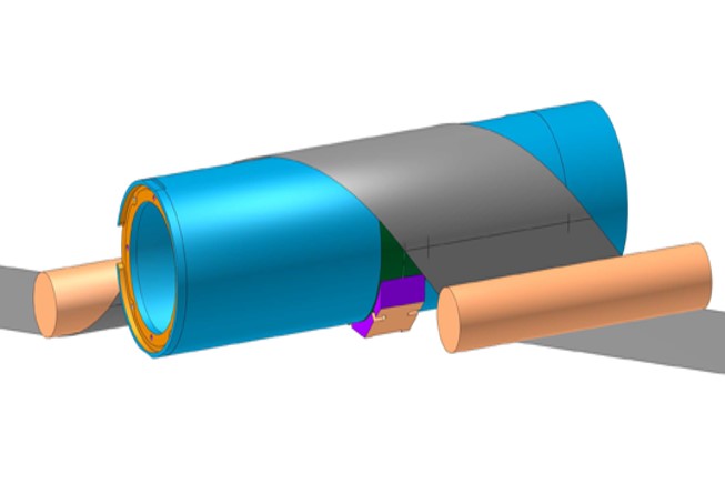
We discuss the feasible shape and structure of the prototype using 3D CAD
“Okay, let’s make it.”
After in-house discussions, a prototype is produced for full-scale verification.
Obviously, the first time, everything would not go well….
“No, this is no good either…”
Some of the prototypes are stored in the supply room.
Various prototypes are built and verified, and data is accumulated to examine and overcome the numerous obstacles that arise each time.
Verification is required not only from the optical system but also from the physical point of view of the conveying base material.
In recent years, we have been rumored to be pursuing elements other than optics exclusively…?
■ It finally started to take shape.
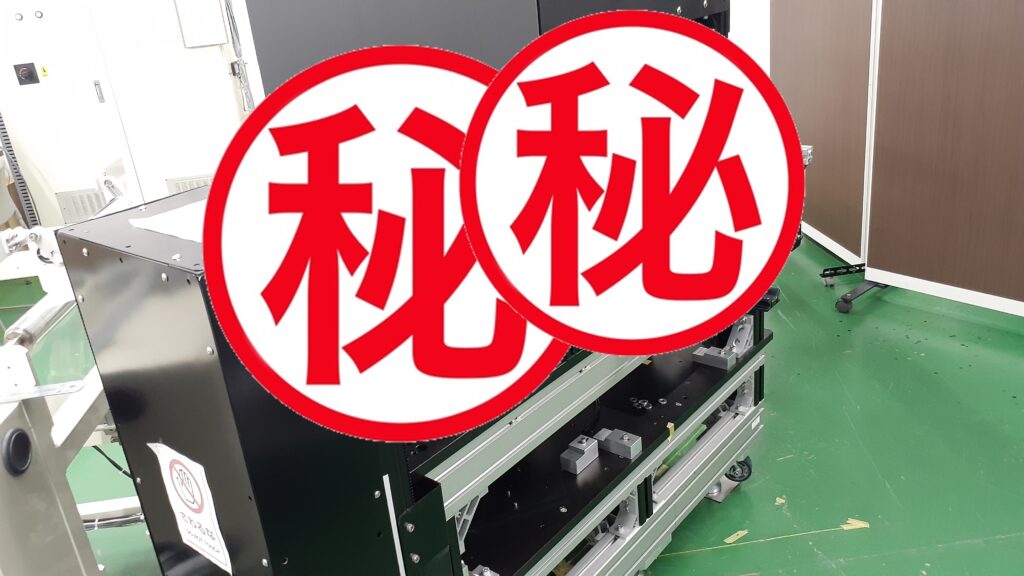
After much struggle and hardship, the device is finally ready to be used.
However, at Wired, we continue to improve our products day by day to make them “better.”
The engineers’ continuous challenge is endless.
“By the way, what is this ㊙ mark?”
“I’m afraid I can’t reveal it to the outside because of confidentiality concerns.”
“That is okay to show it. It is not a scene from a hot spring bath.”
